Every aspect of an electronics project is covered
PCB Design & Layout: Advanced PCB design & layout up to 12 layers with buried via's can handle any PCB project you need. Expert layout done by electronics engineers who understand layout parameters. Don't spent time on a production layout before you have verified; Net List verification, component selection, design, component PCB package. Add Software Test Points to aid software development...then layout the production board. 
|
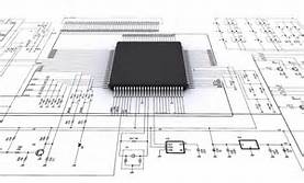
Electronics Design:
Every aspect of analogue & digital design from prototype through development boards to final production:
Embedded Software: Embedded software development in ANSI-C.
|

I use the most popular PCB Applications for your project...
P-CAD allows us to export Net-List files and import them into our Cadence High Speed Routers. The completion rate is always 100% because we relax the routing rules. Once everything has been fully verified and Test Coded, we switch to Altium.
Altium is used for the final PCB layout because of its CAD support structure and precision. |

'Altium Designer' is the property and trademark of Altium Software
|